Sputtertalk
Join us as we explore the frontlines of innovation in experimental & applied engineering research. In each episode, we share insights from industry and academic professionals with experience working on real, impactful, projects. Listen to Sputtertalk for grounded conversations about building systems that matter.
Latest Podcast Episodes
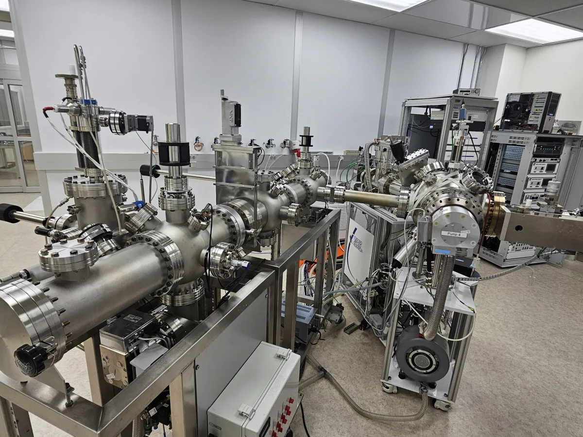
Meet Nanosys2
Meet Nanosys 2
Six chambers, five roughing pumps, three turbomolecular pumps, one ion pump, several hundreds of screws and bolts, and many, MANY, cooling lines. This is Nanosys 2 - a horizontal foundry for nanocluster depositions using both magnetron sputtering (physical vapor deposition) and plasma-enhanced chemical vapor deposition (PECVD) at UNLV's SEB cleanroom to create specialized materials, devices, and nanostructures.

This article will be a bit more technical than the others, but it's one I've really wanted to write. In short, we use this amazing contraption to grow specific materials in incredibly thin layers, layer by layer, and with nanometer-precision (or as close as we can get!). The research Nanosys 2 helps conduct can generally fall into three categories:
Generating novel materials to study their properties and learn their characteristics.
Studying the process of growing materials with useful characteristics.
Taking materials with known useful characteristics and coating specialized devices with them to achieve a certain functionality.
The system is designed for two- and four-inch wafers and can take as many as eight in a single process run. Wafers are chosen with the growth material and desired end-geometry in mind. The first step to any process run (assuming your chosen target is already prepped!) is loading the wafers into the entry port. After sealing them in the first chamber, we begin pumping the internal pressure down to at least 10⁻⁴ Torr using roughing (stage 1) pumps. Once that pressure is achieved, we can turn on the more capable (but more fragile) pumps to bring the pressure down even further. The pressure inside each chamber will fluctuate a few times depending on the process, cyclically, to achieve certain goals. Our first goal is to remove any contaminants, sometimes that involves baking the system out to around 300°C using external heaters. Other times it involves blasting contaminants off the wafers using even hotter elements.

An important thing to note here is the controlled nature of modifying the internal chamber pressure. Modifying the pressure too quickly, either by venting gasses into the system at high pressure or turning the turbo and ion pumps on too early, can permanently damage the system - possibly irreparably. The pressure is, of course, negative. We never pump more gas into the system than what would raise the internal pressure to atmosphere. How much positive pressure in standard atm could the system withstand internally?
After cleaning the wafers and doing any pretreatments necessary, the wafers, one at a time, are moved into the main deposition chamber for whatever material growth we have destined for it. This is done using transfer arms that have specialized bearings, allowing us to manipulate the cart and wafers externally without breaking vacuum. The process of transferring a wafer from the cart to the first transfer arm, then to the interchamber transfer arm, and onto the wafer holder in the main chamber is quite tedious, but rewarding. The same process must be done in reverse to extract the wafer from the system post-deposition.
The chambers are all connected linearly and sequentially, with one special PECVD chamber attached off chamber #1. The final chamber is the nanocluster deposition chamber, and it connects directly to the main deposition chamber. Essentially an elongated tube, a magnetron sputterer sits on one end with a target attached to it, and a quadruple mass filter (QMF) on the other end to filter out specific nanoparticle cluster sizes heading towards the wafer/device. This filtering is accomplished by applying electric fields at certain voltages and frequencies along the deposition path.
Another aspect of filtering is gas introduction. Helium injected in small quantities is used to either aid or inhibit nanocluster formation - i.e. creating bigger or smaller particles. Setting the sputterer closer or further away from the QMF (the aggregation length) alters how much time the particles have to collide and cluster as well. There's a delicate balance to be made and many parameters that can drastically alter your results. Say, for example, if you set the aggregation length far too short, your nanoparticles can focus around a really small area instead of uniformly spreading across your wafer, and you'll get this:

This was my first-ever deposition, generating gold nanoparticles. Dear reader, if you are embarking on the journey that is preparing and conducting your first deposition and thin film growth experiment, use something less valuable than gold!
Sputtering
In addition to the helium, argon gas must be present to facilitate the generation of plasma on the surface of the magnetron sputterer's target. Often a ratio of 75% argon to 25% helium produces good results for the standard procedures we conduct. For some of my research, I introduce nitrogen gas to generate an effect called "reactive" sputtering, but that is a topic for another article. Here is a picture of the magnetron sputterer/nanocluster deposition source.

You would never usually see it like this - we brought the device out to service it. At the top is a set of electrically isolated shells that hold the target - your desired sputter material, like AlN, AlGaN, Au, for example. That isolation is crucial, as the entire process hinges on the generation of stable plasma through the presence of argon gas and a strong electric field. Typically, we do experiments with metals that conduct electricity well, and therefore use a DC power source. When using nonconductive or semiconductive targets, like nitride-based targets, DC power sources would fail. Plasma would not generate as the target does not conduct electricity to the target holder base, and instead accumulates charge on its surface. If done without diligence and care, the charging can burn through the target and destroy the target holder itself. In our system, cooling water lines run directly behind the target, and damage to the target holder could potentially leak water into the sputter chamber. Needless to say, that would be catastrophic.
There are shields, processes, and equipment in place that would all have to be bypassed to reach that point, but it is a distinct and dangerous possibility. Thus, for such targets, we generally use AC power sources that clear charge accumulation on their negative half-cycle. Typically RF frequencies accomplish this well, though at low deposition rates. Some other situations require nuance, like reactive sputtering using a metallic target in the presence of a certain gas. Here, something called target poisoning and consequent charge accumulation can still occur, though an AC power source is not entirely desirable or necessary (in part due to the cost, setup, and low deposition rate). Instead, we'd use a pulsed-DC power supply featuring a programmable negative portion of the cycle (isn't this really just AC?) to clear the charge accumulation and prevent poisoning, though the frequency isn't nearly as high as an AC source and thus it has its limits.

Completing the Process
You've made it this far. Your gas ratios are adjusted nicely, you can tell your plasma generation is stable based on the current readout on your power supply, some deposition is detected on your rate/thickness monitor. Now begins the experimentation, as by now, you would've set some parameters on your QMF with the expectation of it filtering out the undesired cluster sizes. You notice the deposition rate is stable on your monitor, and you move your internal baffles to direct the particle flow to your wafer. Depending on the material, you've either applied heating or cooling to your wafer using the wafer holder's internal mechanisms, possibly applied a large bias to attract particles.
After hours of setup, days of waiting for proper vacuum pressure, thermally cycling the chamber to eradicate those pesky trace water molecules and universe-forbid any oils, you conduct your experiment.
It lasts ten-twenty minutes.
Almost a week of setup, for ten minutes. That's it. Ramp down the power on the supply, stop gas flow, program the turbo pumps to fully ramp down, equalize the pressure across the transfer chambers, and spend an hour trying to transfer your wafer back to the wafer cart without dropping it to the bottom of the deposition chamber where it will surely shatter into countless fragments. If you set up additional wafers, repeat this process for each of those, though your setup will be a bit shorter thankfully.
Fortunately, this has been conducted in an ISO-certified cleanroom, and though particulates are still flowing through the air of the room, you're able to transfer your wafer(s) to the appropriate characterization equipment to analyze the deposition geometry, particle size, or electrical parameters. Take care not to destroy your samples in this process (like through charge accumulation on an SEM-EDX machine)!
I know I brushed over many technical aspects of this, and probably explained more than what was necessary for a few portions. If you feel there's something I've explained incorrectly here, or you'd like to know more, please reach out to me! I'd take any chance to discuss my research work and/or get feedback on it.
Thanks for the read, and happy researching.

Subscribe to the Podcast
COMPANY
EXPLORE
CUSTOMER CARE
LEGAL
© Copyright 2026. Danny Benjelloun. All Rights Reserved.